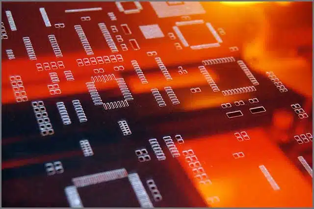
Precision is essential when it comes to making printed circuit boards (PCBs). The stencil is an important tool in the PCB manufacturing process since it helps to apply solder paste to the board precisely. A well-made PCB stencil guarantees uniform solder paste deposition, which results in dependable and high-quality PCB assemblies. In this post, we’ll go over the steps for making a PCB stencil in great detail.
How do you Create a PCB stencil?
Creating a PCB stencil by the pcbasic a leading manufacturer involves several intricate steps. Let’s walk through the process, highlighting key aspects along the way:
Understanding the Basics
Before we go into the manufacturing process, let’s go over the fundamentals of a PCB stencil. A stencil is often composed of a thin metal sheet, most often stainless steel. It features precise apertures corresponding to the solder paste deposition points on the PCB. These apertures allow the right amount of solder paste to be applied, ensuring accurate and consistent soldering.
Designing the Stencil
The first step is to design the stencil itself. This is done using specialized PCB design software. The design includes the pattern of openings that match the soldering points on the PCB. The stencil design must align perfectly with the PCB layout to ensure precise solder paste application.
Material Selection
It’s essential to choose the appropriate material for the stencil. Stainless steel is commonly used because of its longevity and ease of cleaning, The thickness of the stencil is determined by the magnitude of the components and the consistency of the solder paste. For larger components, thicker stencils are employed, whereas smaller, more intricate components are employed with finer stencils.
Laser Cutting or Chemical Etching
Once the stencil design is ready, it’s time to manufacture it. Stencils can be created through two main methods: laser cutting or chemical etching. Laser cutting is a quicker method that involves using a laser beam to precisely cut the openings in the stencil. Chemical etching, on the other hand, involves applying a chemical solution to selectively remove metal and create the openings.
Applying a Surface Finish
After the stencil is cut or etched, a surface finish is applied. This finish helps prevent oxidation and ensures smooth solder paste release. Nickel and gold are commonly used finishes due to their conductivity and anti-oxidation properties.
Quality Control
Before the stencil is put into production, thorough quality control is essential. Inspecting the stencil for any defects or inconsistencies ensures that the solder paste will be accurately deposited during the PCB assembly process.
Storage and Handling
Stencils are sensitive and must be stored and handled with care. To avoid damage or illness, keep stencils in a clean and dry environment. It is critical to handle the stencil with care in order to avoid harming or bumping its surface.
Expert Tips from PCBASIC for Successful PCB Stencil Creation
- Precision is Paramount: Accurate stencil design and manufacturing are crucial for high-quality PCB assemblies. Even a minor misalignment can lead to soldering issues.
- Consider Component Sizes: Choose the appropriate stencil thickness and aperture sizes based on the components’ sizes. This ensures optimal solder paste application.
- Opt for Professional Manufacturing: While DIY stencil kits exist, it’s recommended to opt for professional stencil manufacturing services to ensure precision and reliability.
- Regular Maintenance: If you’re using stencils for repeated production runs, regular maintenance and cleaning are essential to prevent clogging of apertures.
- Collaboration with PCB Designers: Effective communication between PCB designers and stencil manufacturers is vital to ensure the stencil design aligns perfectly with the PCB layout.
FAQs
How much time does it need to make a PCB stencil?
The time needed to make a PCB template relys on the complexity of the design. Additionally, it depends on the making method and lead time selected by the company. Usually, It takes a few days to a few weeks to fully re-grow.
Can I reuse a PCB stencil for multiple projects?
Yes, you can reuse a PCB stencil for multiple projects, especially if they share similar components and layouts. However, regular maintenance and cleaning are essential to ensure consistent solder paste deposition.
Are DIY stencil kits effective?
DIY stencil kits can be effective for simple projects or prototypes. However, for professional and production-grade PCB assemblies, it’s recommended to opt for stencils manufactured by professionals. These stencils offer higher precision and durability.
What is the cost of PCB stencil manufacturing?
The expense of manufacturing PCB’s via stencils is based on the size of the stencil, the method of manufacturing chosen, and additional features like surface quality. Typically, the expense is between tens to a couple of hundred dollars.
Can I adjust the stencil thickness for different components?
Yes, you can adjust the stencil thickness based on the components’ sizes. Thicker stencils are suitable for larger components, while finer stencils are used for smaller components and finer pitch designs.
How do I clean a PCB stencil?
To clean a PCB stencil, use a specialized stencil cleaner and a lint-free wipe. Gently remove any solder paste residues from the apertures. Avoid using abrasive materials that could scratch the stencil surface.
Conclusion
Creating a stencil from a PCB is crucial to the manufacturing process for PCBs. With exactness, attention to detail, and a collaborative effort between PCB designers like pcbasic and stencil manufacturers, you can guarantee the consistent and accurate application of solder paste. Whether you’re dealing with a prototype or a large volume production, a well-designed PCB stencil is a crucial component that enhances the quality of your entire PCB assemblies.
Lucas Noah, armed with a Bachelor’s degree in Information & Technology, stands as a prominent figure in the realm of tech journalism. Currently holding the position of Senior Admin, Lucas contributes his expertise to two esteemed companies: OceanaExpress LLC and CreativeOutrank LLC. His... Read more